|
Radio Modifications |
|||||||||||||||||||||||
 |
Realistic DX-394Noise Blanker Mods |
|||||||||||||||||||||||
| Introduction
Those who have used the noise blanker button will note that it has no apparent effect on the interference. This is because it is designed to be proof against "impulse-type" noise such as may be heard on an AM radio in a car. These wide-band products mix so well with the wanted signal that they become a part of it. While the noise blanker circuit can help reduce noise it cannot eliminate all the noise products and can introduce some audio distortion. It has been reported that the stock performance on AM is marginal at best and it just doesn't work at all on CW/SSB. The modifications will improve the AM noise blanker performance and allows it to work fully on CW/SSB. |
||||||||||||||||||||||||
| Circuit Diagram | ||||||||||||||||||||||||
 Noise Blanker Input Stage |
||||||||||||||||||||||||
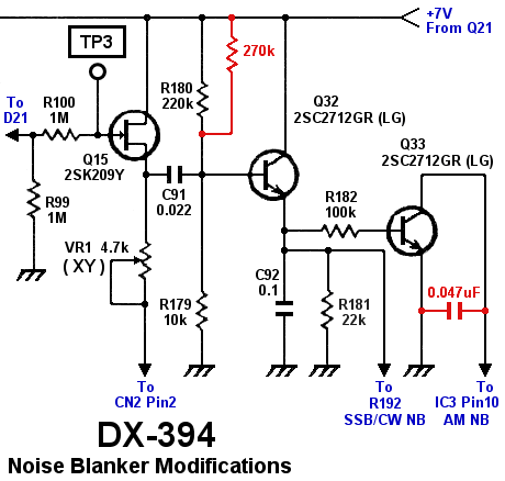 Noise Blanker Output Stage |
||||||||||||||||||||||||
|
||||||||||||||||||||||||
| Procedure | ||||||||||||||||||||||||
 |
||||||||||||||||||||||||
| Removal
of the surface mount ceramic capacitor C43 and the fitting of a standard
100pF ceramic capacitor and a 4.7k resistor is performed during the
455kHz IF modifications. Solder a 0.1uF (104) ceramic capacitor across R91 and C86. |
||||||||||||||||||||||||
 |
||||||||||||||||||||||||
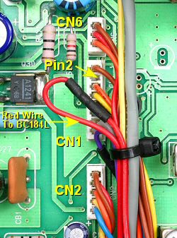
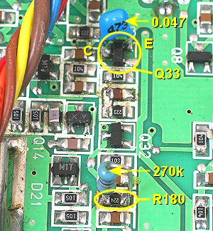
| Place
a 270k 0.6W standard resistor across the 220k surface mount resistor
R180. Solder a 0.047uF (473) ceramic capacitor across the Collector and Emitter of Q33, see photo. |
||||||||||||||||||||||||
bhi DSP AM Noise Blanker Modifications |
||||||||||||||||||||||||
| After
installing the DSP module you will notice a reduction in the
effectiveness of the AM noise blanker. This is because audio muting is
applied within the input stage of the audio power amplifier IC4 and not
IF muting like in the SSB product detector. The DSP module is introduced
between the output of the audio preamplifier transistor Q28 and the
input of the power amplifier IC4. A Digital Signal Processor converts
the analogue audio signal into a digital representation. It
differentiates the speech from the noise. The unwanted noise and
interference is then attenuated to leave only the speech. This digital
signal must be converted back into an analogue signal. The conversion
and processing takes time, so the audio signal is delayed from reaching
the power amplifier. This time delay will still occur even if you
deselect the noise cancellation. The noise blanking pulses fed to pin 4
of IC4 are out of step with the delayed audio from the DSP module. To
correct this the blanking pulses must be applied to a muting circuit
before the DSP module. Fortunately one already exists in the DX-394. IC3
a Quad Bilateral Switch (TC4066F) is used to select the audio path for
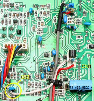
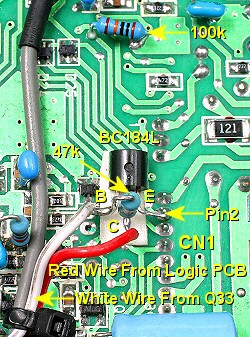
each mode, AM, SSB and CW. By simply adding a transistor switch (BC184L)
controlled by the noise blanking pulses the control pin of the AM
section of IC3 (pin 13) will mute the audio signal before entering the
DSP module. |
||||||||||||||||||||||||
| Circuit Diagram | ||||||||||||||||||||||||
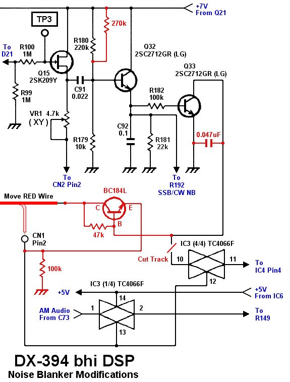 Noise Blanker Output Stage and AM Muting |
||||||||||||||||||||||||
|
||||||||||||||||||||||||
| Procedure | ||||||||||||||||||||||||
|
||||||||||||||||||||||||
| Back | ||||||||||||||||||||||||